- 您现在的位置:买卖IC网 > Sheet目录346 > NCP5010FCT1G (ON Semiconductor)IC LED DRVR WHT BCKLT 8-FLIPCHIP
NCP5010
V bat
2.7 to 5.5 V
C in
4.7 m F 0603
X5R 6.3V
L1
22 m H
LED
ENABLE
A2
A3
CTRL
NC
V OUT
C1
C out
1 m F 0805
X5R 25V
LED
NCP5010
R fb
24
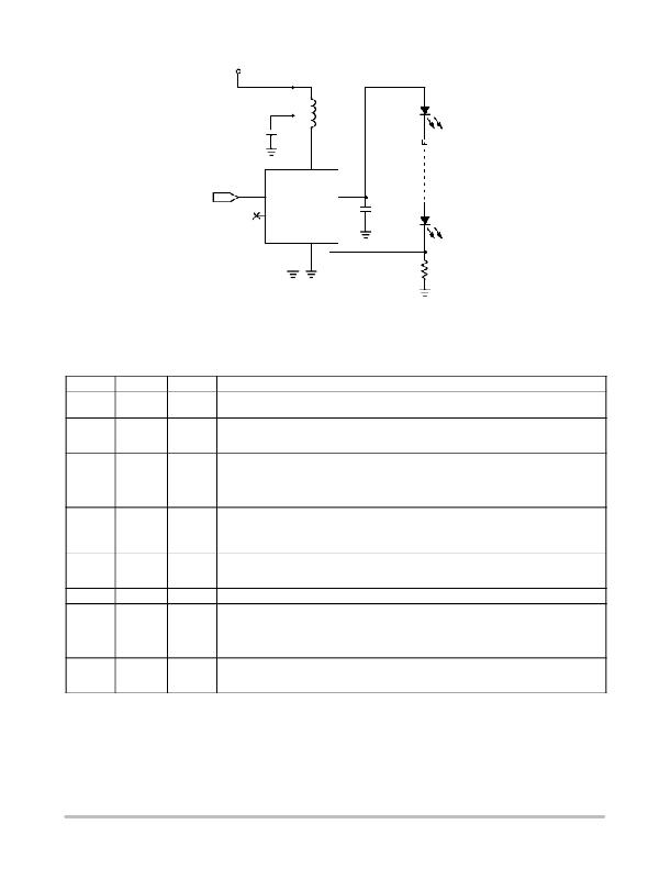
Figure 2. Typical Application Circuit
PIN FUNCTION DESCRIPTION
PIN
A1
PIN NAME
AGND
TYPE
POWER
DESCRIPTION
System ground for the analog circuitry. A high quality ground must be provided to avoid spikes and/
or uncontrolled operations. This pin is to be connected to the PGND pin.
B1
V IN
POWER
Power Supply Input. A ceramic capacitor with a minimum value of 1 m F/6.3 V (X5R or X7R) must be
connected to this pin. This capacitor should be placed as close as possible to this pin. In addition,
one end of the external inductor is to be connected at this point.
C1
V OUT
POWER
DC?DC converter output. This pin should be directly connected to the load and a low ESR
(<30 m W ) 1 m F (min) 25 V bypass capacitor. This capacitor is required to smooth the current flowing
into the load, thus limiting the noise created by the fast transients present in this circuit. Since this is
a current regulated output, this pin has over voltage protection to protect from open load conditions.
Care must be taken to avoid EMI through the PCB copper tracks connected to this pin.
A2
CTRL
INPUT
An Active High logic level on this pin enables the device. A built?in pulldown resistor disables the
device if the pin is left open. This pin can also be used to control the average current into the load
by applying a low frequency PWM signal. If a PWM signal is applied, the frequency should be high
enough to avoid optical flicker but be no greater than 1 kHz.
C2
SW
POWER
Power switch connection for inductor. Typical application will use a coil from 10 m H to 22 m H and
must be able to handle at least 350 mA. If the desired output power is above 300 mW, the inductor
should have a DCR < 1.4 W .
A3
B3
NC
FB
N/A
INPUT
Not Connected
Feedback voltage input used to close the loop by means of a sense resistor connected between the
primary LED branch and the ground. The output current tolerance is depends upon the accuracy of
this resistor and a ± 5% or better accuracy metal film resistor is recommended. An analog dimming
signal can be applied to this point to reduce the output current. Please refer to the application
section for additional details.
C3
PGND
POWER
Power ground. A high quality ground must be used to avoid spikes and/or uncontrolled operation.
Care must be taken to avoid high?density current flow in a limited PCB copper track. This pin is to
be connected to the AGND pin.
http://onsemi.com
2
发布紧急采购,3分钟左右您将得到回复。
相关PDF资料
NCP5021MUTXG
IC WHITE LED DVR HV AMB 16-UQFN
NCP5050MTTXG
IC LED DRIVR PHOTO FLASH 10-WDFN
NCP5111DR2G
IC DRIVER HI/LOW SIDE HV 8-SOIC
NCP5304DR2G
IC DRIVER HI/LOW SIDE HV 8-SOIC
NCP5355DG
IC DRVR SYNC BUCK MOSF 12A 8SOIC
NCP5359ADR2G
IC MOSFET GATE DVR DUAL 8-SOIC
NCP5359DR2G
IC GATE DRIVER VR11.1/AMD 8-SOIC
NCP5360RMNR2G
IC DRIVER MOSFET 56QFN
相关代理商/技术参数
NCP502
制造商:ONSEMI 制造商全称:ON Semiconductor 功能描述:80 mA CMOS Low Iq Voltage Regulator in an SC70−5
NCP502 K20PA WAF
制造商:ON Semiconductor 功能描述:
NCP502/D
制造商:未知厂家 制造商全称:未知厂家 功能描述:80 mA CMOS Low Iq Voltage Regulator in an SC70-5
NCP502_07
制造商:ONSEMI 制造商全称:ON Semiconductor 功能描述:80 mA CMOS Low Iq, Low−Dropout Voltage Regulator
NCP5021
制造商:ONSEMI 制造商全称:ON Semiconductor 功能描述:High Voltage White LED Driver with Ambient Light Sensing
NCP5021MUTXG
功能描述:低压差稳压器 - LDO NCP5021 RoHS:否 制造商:Texas Instruments 最大输入电压:36 V 输出电压:1.4 V to 20.5 V 回动电压(最大值):307 mV 输出电流:1 A 负载调节:0.3 % 输出端数量: 输出类型:Fixed 最大工作温度:+ 125 C 安装风格:SMD/SMT 封装 / 箱体:VQFN-20
NCP502ASQ15T1
制造商:ONSEMI 制造商全称:ON Semiconductor 功能描述:80 mA CMOS Low Iq Voltage Regulator in an SC70−5
NCP502ASQ15T1G
制造商:ONSEMI 制造商全称:ON Semiconductor 功能描述:80 mA CMOS Low Iq, Low−Dropout Voltage Regulator